Research background
People usually refer to the phenomenon that the conductive capacity of a semiconductor changes with the electric field as "field effect".
The transistor is regarded as one of the greatest inventions of mankind in the 20th century. In 1930, Lilienfeld proposed that by applying a strong electric field to the surface of the semiconductor to generate a current, and can be like a water valve by changing the strength of this electric field to control the size of the induced current. This is the first interpretation of the operation of the field effect transistor. After 30 years, Bell LABS successfully prepared the first silicon basic-oxide-semiconductor field-effect transistor (MOSFET) on Si/SiO2, and this information was released at the solid-state physical device research conference, which ushered in the attention of many manufacturers and researchers, followed by the maturing of research. In 1961, the Radio Corporation of America research team found that transistors can be prepared by evaporation of semiconductor materials on the base of a postage stamp size, thus proposing the concept of thin film transistors, this discovery not only greatly improves the integration of transistors, but also effectively promotes the development of organic thin film transistor OTFT. In 1986, the polythiophen-based field-effect transistor, recognized as the first organic thin film transistor device, was successfully developed and reached the performance standards that can really work effectively in organic circuits. Since then, through a variety of optimization methods, such as new synthetic materials, new preparation methods, new interface engineering, etc., the research progress in this field can be described by leaps and leaps, all aspects of performance parameters have been changing with each day, a variety of products have been widely used in the manufacture of large-scale complementary integrated circuits, flat panel display driver circuits, various sensors and so on.

Canonical study
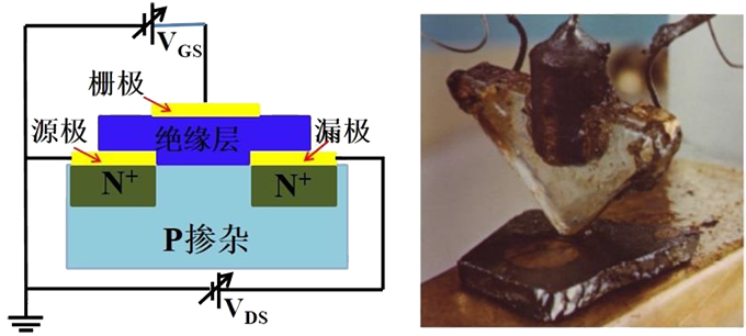
A typical FET can be viewed as a flat plate capacitor consisting of a gate and an active layer that can control the carrier concentration in the channel through the voltage across the gate. When the gate-source voltage VG is applied, the induced charge will be generated near the interface of the insulation layer, and under the action of a certain external source-drain voltage VSD, the induced charge will participate in conduction along the conductive channel, which greatly changes the resistivity of the semiconductor material. Therefore, the electric field intensity between the gate and the active layer is adjusted by adjusting the gate-source voltage VG, so as to change the density of induced charge in the active layer, and then the source drain current ISD also changes, and finally the effect of controlling the source drain current ISD by adjusting the gate source voltage VG. Figuratively speaking, this control relationship is like a water valve regulating the flow of water (source and drain current) through the valve (gate).
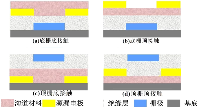
Transistors can be roughly divided into four categories by the location of the gate, insulation, source leakage and channel layers.
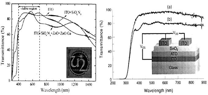
Transparent field-effect transistors (Fets) were reported in 2003 and are mainly made of ZnO materials. Due to the significant application prospect in the display, organic and inorganic active layers are prepared by electrochemical polymerization, molecular self-assembly, magnetron sputtering, CVD and other methods, and the insulation layer represented by SiO2 is produced, so as to manufacture transparent field-effect transistors based on glass substrates.
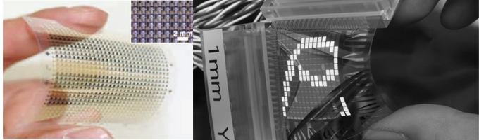
Inorganic transistors can only be displayed in a flat way, and can not do a very flexible bending display, while organic thin film transistors can be bent and stretched arbitrarily because of the use of organic materials, which truly liberates the flexibility of the flexible substrate, and many new applications can be born. For example, it can be made on a flexible substrate to become a flexible display.
The research of various new types of marginal materials, such as single root nanomaterials, carbon materials, etc., makes the preparation of high performance transistors possible.
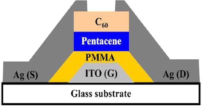
On the one hand, under the action of gate voltage, the insulating layer, as an insulating medium, generates a strong electric field to induce conductive contact at the interface between the insulating layer and the semiconductor layer. On the other hand, it is in direct contact with the semiconductor layer. The surface condition of the insulating layer, such as roughness and defects, greatly affects the growth form and carrier transmission of the semiconductor layer. By modifying the insulation layer, the properties of the transistor can be effectively adjusted.
The choice of electrode material is related to the performance of the transistor, and also determines the compatibility of the preparation process.
Devices based on single root materials and some nanomaterials are one of the current research hotspots.
Various gas sensors, humidity sensors, piezoelectricity and photoelectric devices based on field effects can improve the characteristics of the devices themselves and provide references for the integration of devices and circuits.
Equipment recommendation
1. Mechanical and environmental controllable flexible FET integrated characteristic analysis platform
AES-4SD flexible electronic device comprehensive test platform: suitable for flexible FET device gas sensitive, humidity sensitive, photosensitive, stress-strain and other comprehensive characteristics of performance analysis, especially support the device electrical characteristics and mechanical characteristics of synchronous analysis; The platform provides precise stretching and extrusion control, as well as simultaneous electrical performance analysis and mechanical monitoring. Configure DC dual source meter to support the research of transistors and other devices; Static valve module is configured to support liquid evaporation valve or gas dilution valve; Equipped with LED light source module, it can be used for photosensitive, photoelectric, photosensitive gas sensitive and other characteristics research; Equipped with CCD or camera to take pictures and video, real-time record the shape changes of materials and devices; It can be connected with an external humidity controllable gas-liquid distribution system, which can accurately control the atmosphere and humidity of the sealed chamber, and is used for the research of gas sensitivity, humidity sensitivity and other related characteristics. In addition, the system is suitable for a variety of flexible materials (graphene, conductive polymers, hydrogels, liquid metals, etc.), flexible devices (sensors, detectors, batteries, capacitors, electronic skin, OLED, etc.) in the stretching, extrusion, bending and different environmental stimuli (gas, humidity, light, etc.) under the stress strain and electrical characteristics of the analysis.
2. In situ analysis system of integrated characteristics of FET based on micro-cavity
CGS-MT photoelectrical integrated test platform: suitable for millimeter-level field-effect transistor devices or external pad to reach the millimeter-level transistor devices of gas sensitive, humidity sensitive, photosensitive and other comprehensive characteristics of the analysis, the platform cavity is small, support with Raman spectrometer, microscope, etc., can be used for electrical and spectral or microscope in situ analysis. Through integrated electrical, probe, microcavity and static valve design, the platform can provide accurate electrical detection, flexible probe connection, accurate temperature regulation and convenient atmosphere control. Integrated dual-source table test system, support two-wire or four-wire test, support dual-channel test; The platform contains an in situ high temperature platform that can be used in combination with Raman spectrometer or microscope to perform spectral or microscopic in situ analysis while conducting electrical testing. The micro-chamber structure of the platform is especially suitable for connecting the humidity controllable gas-liquid distribution system, which can realize the rapid replacement and balance of the atmosphere concentration and humidity in the chamber, and can be used for the online detection of gas and humidity sensitivity. Platform support with LED light source or external light path, photosensitive, photoelectric, photosensitive gas sensitive and other related research; The platform supports the connection of vacuum pumps for performance testing under vacuum or different air pressures. In addition, the platform is also suitable for in-situ testing and comprehensive characteristic analysis of a variety of millimeter-level materials (semiconductor oxides, graphene, carbon nanotubes, conductive polymers, etc.) or devices (sensors, detectors, transistors, etc.).
3. Integrated characteristic analysis system of transistor devices with precision probe station and environmental control
AES-4TH Environment Controlled Probe Test platform: It is suitable for the comprehensive characteristic analysis of transistor-based devices that require probe precision regulation and environmental simulation. The platform is designed through integrated electrical detection, microprobe connection, environmental control, microscope observation, and overall shielding, shock-proof and anti-interference processing. Provides precise electrical inspection down to the pA level, micrometer level precision probe regulation, wide range of highly stable ambient humidity and hot station temperature control. The platform adopts multi-probe connection and bottom gate design, which is especially suitable for comprehensive characteristic analysis of FET devices. At the same time, the platform provides temperature and humidity regulation, which provides an environment for measuring the temperature characteristics and humidity resistance characteristics of the transistor. The platform with a vacuum pump can support the research of device characteristics under vacuum conditions, the external light source or the built-in optical fiber can support the research of photoelectric, photoconductive, photosensitive gas sensitive and other characteristics of the device, and the humidity controllable gas-liquid distribution system can support the research of gas sensitive, humidity sensitive, humidity resistant and other characteristics of the device. The open interface reserved for the platform can be combined with electrochemical work or impedance analyzer for multi-signal measurement. In addition, the platform is suitable for comprehensive characteristic analysis of related materials or devices that require precise probe connections and environmental conditions.
Typical result
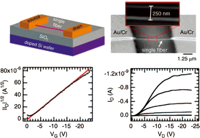
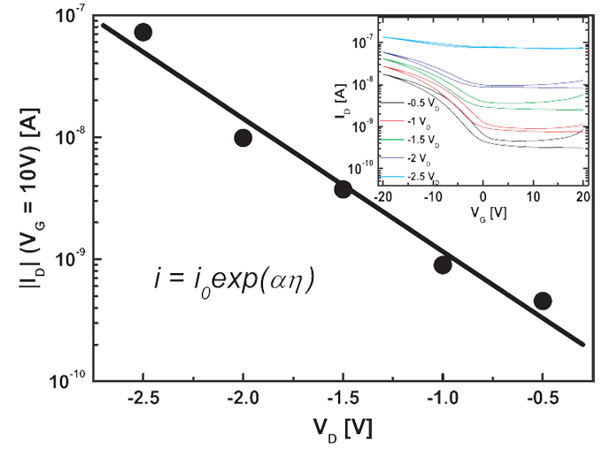
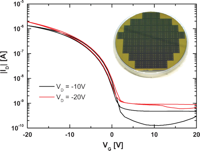
The output characteristic curve is used to describe the relationship between current Id and voltage Vd when Vg takes a certain value, reflecting the influence of drain-source voltage Vd on Id.
The transfer characteristic curve reflects the control effect of gate-source voltage Vg on Id.
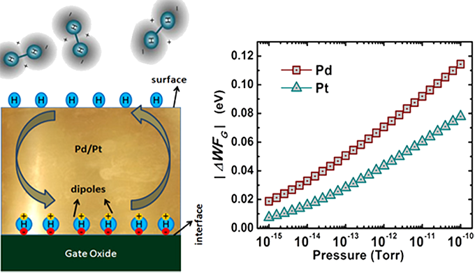
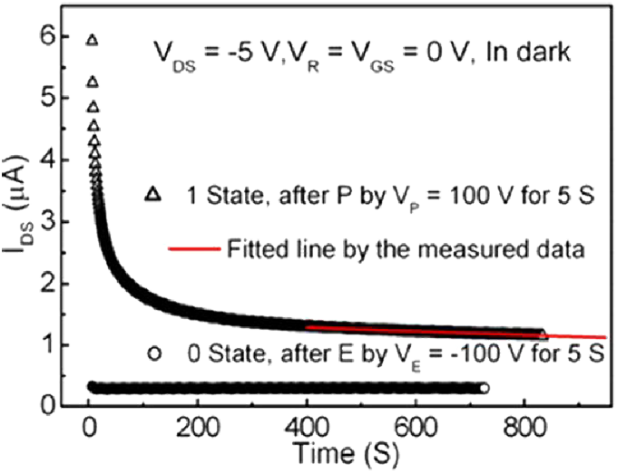
Data retention ability is an important parameter of non-volatile storage, and the test device can reflect the speed of decay under the influence of objective conditions such as humidity, oxygen and temperature in the environment.
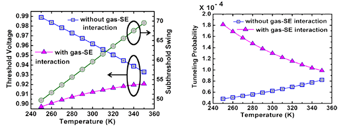
The ID-VD curves at different temperatures are measured to determine the dependence of device performance on temperature.
Absorption spectra are used to describe the transmittance of a device.
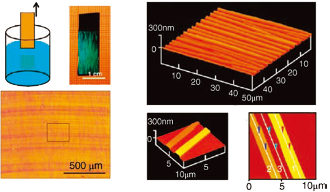
SEM, TEM, and AFM diagrams are used to illustrate the surface characteristics of the insulation layer.
reference
L. Mai, Y. Dong, L. Xu, C. Han, Single Nanowire Electrochemical Devices, Nano Lett., 2010, 10, 4273-4278.
L. Guo, Z. Zhong, Y. Wang, Atomic Layer Deposition on Block Copolymer Membranes with Gyroidal Nanopores Toward Periodically Nanostructured Vapor Sensors: Nanotubes versus Nanorods, Adv. Mater. Interfaces, 2016, 1600017.
D. Natali, M. Caironi, Charge Injection in Solution-Processed Organic Field-Effect Transistors: Physics, Models and Characterization Methods, Adv. Mater., 2012, 24, 1357-1387.
T. Someya, A. Dodabalapur, J.Huang, K.C. See, H.E. Katz, Chemical and Physical Sensing by Organic Field-Effect Transistors and Related Devices, Adv. Mater., 2010, 22, 3799-3811.
Y. Guo, G. Yu, Y. Liu, Functional Organic Field-Effect Transistors, Adv. Mater., 2010, 22, 4427-4447.